- C3 UGF Mohan Garden,
Uttam Nagar, New Delhi-110059
- +91 11 43466023
+91 9311960005
- +91 9717421133
+91 9818080510
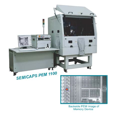
SEMICAPS PEM [Photon Emission Microscope]
SEMICAPS PEM [Photon Emission Microscope]
DESCRIPTION:
SEMICAPS Photon Emission Microscope (PEM) is a failure analysis technique for localization of defects in semiconductor devices. Capable of quickly locating leaky junctions, contact spiking (due to ESD), latch-up, oxide breakdown, and other current leakage phenomena that produce light emissions.
System sensitivity plays a pivotal role in photon emission and is imperative for detection of the faint emissions. SEMICAPS recognizes this important and essential requirement and we offer a high performance, highly sensitive system, that is unmatched when it comes to sensitivity.
CRITICAL DESIGN CONSIDERATIONS
Optics
SEMICAPS designs to optimize and enhance the system for maximum photon throughput to the detector.
High Numerical Aperture & Long Working Distance Objectives Lens
The NA of the objective lens is critical. Higher NA lens yield better light collecting efficiency. Long working distance lens have better depth of focus and allows microprobing of devices
High Sensitivity Macro Lens
To provide a global view of the entire device, SEMICAPS offers 1x macro lens with a high NA of 0.4.
Optimized Tube Lens Design
For maximum light throughput, SEMICAPS PEM uses large diameter tube lens to minimize light loss and prevents vignetting, thus improving sensitivity.
HIGHLY AUTOMATED SYSTEM
The SEMICAPS PEM series have been designed for high automation of hardware and software and also the ability to switch over to manual control when desired.
Computer Controlled XYZ Stage
Stage movement is fully controlled from the computer console via the X, Y and Z buttons on the software or by joystick control. A rapid image shift is enabled by double-clicking on the image displayed live on the window.
Motorized Optics
Detectors and optics are automatically moved into and out of position from the optical path depending on the imaging mode (Live or Capture) chosen.
NIR Filter: Key to Backside Imaging
On selecting Backside Imaging, the NIR filter automatically positions into the optical path.
SOFTWARE USER INTERFACE
User-friendly Software SPEMS Windows-based system software includes real-time frontside and backside imaging, image acquisition and overlay, image processing and annotation, image data attachment, thumbnail browsing, pseudo-coloring and other functions that simplify the system operations.
Live Navigation Window
The SEMICAPS SPEMS series enables live stage navigation on the window with its dual camera system. The DUT can be continuously monitored and inspected without opening the light-tight enclosure.
Local Coordinates Registration
A standard feature in the software, the coordinate registration system enables users to interface with almost any third party CAD software (eg, Knights).
Par Center and Par Focus
Par center and par focus are software corrected so that the image center and focus do not change with different objectives.
Image Processing and Annotation
Extensive tools like image processing, annotation and customized data reports are available in the software thus eliminating the need for third party software.
REAL-TIME BACKSIDE IMAGING
With an automated removable NIR filter, optimized optics and light source, SEMICAPS SPEMS series offer both frontside and backside imaging as standard features in one integrated system.
BASIC TECHNICAL DATA:
PEM Camera
Cooled CCD (SPEMS 1350 standard system)
Resolution 1024x1024
Pixel size 13x13um
Back-illuminated CCD
Noise <0.01e- per second per pixel.
Integration time (0.1s to 1 hour)
Peltier cooling (Max -70â—¦C using water circulation)
Wavelength range (400nm to 1.1um)
Cooled CCD (SPEMS 1100 standard system)
Resolution 765x510
Pixel size 9x9um
Front-illuminated
Noise < 0.1e- per second per pixel
Integration time (0.11s to 1 hour)
Peltier cooling (Max -35â—¦C below ambient)
Wavelength range (400nm to 1.0um)
Objective Lens
1x (marco), 2.5x, 5x, 20x, 50x, 100x
Optional - 10x, HR50x, HR100x
Stage/DUT
Standard configuration
XYZ traverse 50mm by 50mm by 100mm
Micro-stepping controller
0.5um step resolution, repeatability 5um for SPEMS1100
0.1um step resolution, repeatability 0.5um for SPEMS 1350
Note: High resolution stage of 20nm resolution and
0.5um repeatability is available as option
DUT holder
6” and 8” Wafer holder.
12” wafer holder (optional)
Custom holder (optional)
InGaAs (optional)
Resolution 320x256
Pixel size 30x30um
Integration time (1ms to 60secs)
Peltier cooling (Max -53â—¦C)
Wavelength range (1.0um to 1.7um)
Computer System
Industrial PC, CPU, 512MB RAM, 80GB HDD, DVD R/W,
3.5" FDD, 4 RS-232 ports Ethernet card, parallel port, USB ports,
keyboard & mouse 17" LCD monitor, Windows (TM) 2000/XP OS
Software
Integrated Windows-based Software, Image Capture Module,
Image Archiving and Browsing, Image Printing, Print Template,
Multiple Image Format Support, Focusing & DUT Positioning,
Advanced Image Processing Module inlcuding Digital Zoom,
Annotation, Brightness, Contrast, Gamma Adjustment, Noise Reduction
(3 levels), Sharpening (3 levels), Smoothing (3 levels), Edge Enhancement
(3 levels), Mosiac, Histogram Equalization
Application:
Main applications for the Photon Emission Microscope is to locate failures like leaky junctions, contact spiking (due to ESD), latch-up, oxide breakdown, and other current leakage phenomena that produce light emissions.
Classifications of Emissions
- Emissions that represent a weakness of the junctions
- Oxide leakage
- Latch-up
- Hot electron
- Emissions that are artifacts of design or test conditions
- Forward/reverse biased diodes
- Saturated MOS transistors
- Floating gates
- Emissions that are non detectable
- Buried junctions
- Non emitting leakage sites
- Ohmic shorts
- Shorted metal interconnects