- C3 UGF Mohan Garden,
Uttam Nagar, New Delhi-110059
- +91 11 43466023
+91 9311960005
- +91 9717421133
+91 9818080510
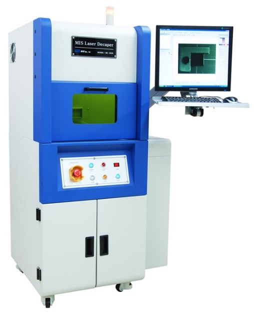
LASER DECAPER
LASER DECAPER
DESCRIPTION:
- Automatic laser decapsulation system
- All types of semiconductor package can be removed
- Any material (Au, Cu, Al) of wire part and 2nd bonding area can be opened
- Effective decapsulation solution for Cu wire chip: Minimize the damage on Cu wire by chemical etching after laser operation
- A few hundred microns of EMC on die surface can be opened with chemical etching (by manual or MIS Wet Etch: Minimal acid use)
- Easy, simple, fast and safe operation
> Vision camera provides real time image
> User can set the decap area by mouse drag / numerical value input
> User can see laser decapsulation process & result on monitor screen
> Superimposing X-ray image on real-time sample picture is available
> Auto door lock : System door is not opened during laser operation
> Automatic Z axis adjustment by PC program - User can observe the operation process through the window (protected from laser radiation)
- Repetitions made simple using recipe files
- Fume & Dust can be exhausted (Option: Fume & Dust collector)
BASIC TECHNICAL DATA:
|
Item |
Description |
|
Laser |
ND YVO4 1064nm |
|
Guide Laser |
632nm Laser Class 2 (Red Beam) |
|
Dimension |
840(W) x 705(D) x 1500(H) mm |
|
Weight |
Approx. 150 kg |
|
Handling IC Size |
2x2 mm ~ 100x100 mm |
|
Vision Camera |
Color |
|
Utility |
Rated Voltage : AC 220V, 1 Phase |
|
Program |
User Interface : Window Based Graphical User Interface |
|
Option |
Fume & Dust Collector |
Applications:
semiconductor has a failure, the first thing is to conduct a non-destructive testing. The non-destructive testing is commonly carried out for an analysis by X-Ray, ultrasound, electrical tests. But for defects that are not detected even by the non-destructive test, destructive testing must be conducted. The first step of the destructive testing in this case is "Decap". The typical semiconductor has a molding with an epoxy to protect the circuit. The operation for the physical and chemical removal of the molding is referred to as "Decap". Mis Laser Decaper Decap is a system that performs this process automatically using laser.